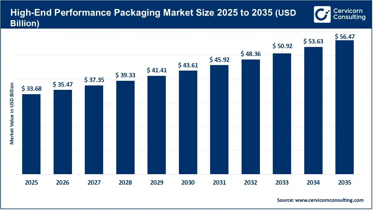
The global high-end performance packaging market size is accounted for USD 35.47 billion in 2026 and is expected to reach USD 56.47 billion by 2035, growing at a CAGR of 5.3% during the forecast period from 2026 to 2035.
- Base Year Market Size (2025): $33.68 billion
- Current Year Market Size (2026): $35.47 billion
- Estimated Year Market Size (2035): $56.47 billion
- Forecast Period CAGR (2026-2035): 5.3%
Report Highlights
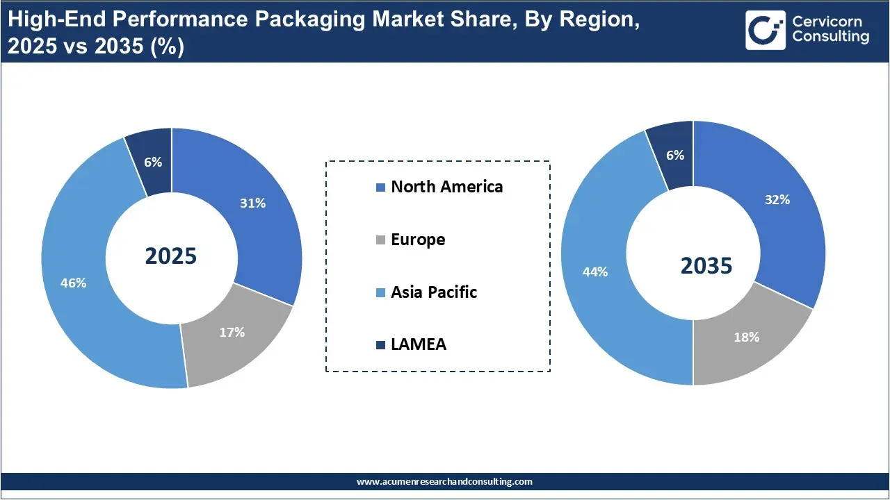
- By region: Asia-Pacific accounted for a revenue share of 45% in 2025 because of its semiconductor manufacturing, assembly, and packaging ecosystem.
- By packaging type: Flip-chip packaging dominated the market in 2025 generated revenue share of 28%, due to its established use in high-performance processors, graphics chips, and networking devices.
- By packaging technology: Through-Silicon Via (TSV) led the market in 2025 (revenue share 27%), driven by its broadened role in high-bandwidth memory and advanced multi-die integration.
- By packaging material: Organic substrates segment registered dominance in the market in 2025 (revenue share 34%), supported by their widespread use in advanced semiconductor packages.
- By application: Artificial intelligence and high-performance computing dominated the market in 2025 (revenue share 32%), fueled by demand for high-bandwidth memory and advanced processor integration.
What are Improvements Covered in the High-End Performance Packaging in 2026?
The high-end performance packaging market includes modern semiconductor packaging technologies that join multiple high-density chips or chiplets with high I/O density of 16 or more I/Os per mm² and a fine I/O pitch of 130 µm or less. Ongoing advances across the industry have pushed several optimizations in 2026, such as hybrid bonding. In addition, leading firms stepped into co-packaged optics (CPO) that recognizes data-throughput and latency risks in larger AI GPU and ASIC clusters. Moreover, breakthroughs have shifted towards customized high-bandwidth memory (cHBM) and the widespread use of system technology co-optimization (STCO).
Recent Significant Funding & Collaborations
- July 2026: The Department of Commerce announced letters of intent with 7 leaders for $874 million to speed up semiconductor R&D for the compute supply chain.
- July 2026: Econovus Packaging, a Pune-based sustainable packaging startup, raised ₹40 crore in a Pre-Series A funding round to support expansion of its engineered packaging solutions across key industrial sectors, like automotive, lithium-ion batteries, solar infrastructure, defence, steel, and broader industrial supply chains.
- July 2026: Amkor Technology, Inc. partnered with NVIDIA to evolve advanced semiconductor packaging and test technologies for next-generation AI and expedited computing platforms.
- June 2026: Taiwan Semiconductor Manufacturing Company and Amkor Technology, Inc. announced a 10-year agreement to promote advanced semiconductor packaging capabilities in Arizona, advancing and fostering investment in the U.S. semiconductor supply chain ecosystem.
Market Dynamics
Market Drivers
- Growth in AI & Integration: The high-end performance packaging market is mainly propelled by higher demand for AI GPUs and ASICs, coupled with a shift toward rigorous multi-die integration, enabling systems to overcome conventional risks and manage vast data throughput.
- Evolution of Hybrid Bonding & CPO: Specifically, hybrid bonding is spurring the development of modern 3D and converged ‘3.5D’ architectures. However, optical engines are expanding rapidly to lower signal loss and latency in accelerated data transfer.
- Prominent Supply Chain Alliance: Along with eventual advances, single AI accelerator packages currently often cover seven or more vendor leaders, which makes early supply-chain co-design a basic need of product development.
Market Restraints
- Supply Chain Checkpoint Issues: Often, to explore advanced packaging, production depends on a handful of regional and corporate gatekeepers, creating a substantial hurdle in the overall process.
- Capacity Differences: Ongoing progressions by OSATs and foundries, like Amkor, are massively seeking 2027–2028, which raises market stress and limitations in the near term.
- Concern in Lead Time & Cost: Many times, companies face challenges in lead times and prices, which pushes engineers to reduce Size, Weight, and Power (SWaP).
Market Opportunities
- Automotive Semiconductor Packaging: Increasing adoption of advanced driver-assistance systems, autonomous driving technologies, and high-performance vehicle computing is creating opportunities for advanced packages designed for demanding automotive environments. Suppliers can develop solutions emphasizing thermal stability, vibration resistance, electrical performance, and long-term reliability.
- Optical Interconnect Integration: Growing data movement requirements in AI infrastructure are creating opportunities for co-packaged optics and other optical-electrical integration approaches. Bringing optical communication components closer to computing chips can help address bandwidth, power consumption, and signal transmission constraints in advanced systems.
- Regional Packaging Capacity: Governments and semiconductor companies are investing in domestic chip manufacturing and supporting supply-chain capabilities. Expanding advanced packaging facilities creates opportunities for equipment suppliers, substrate manufacturers, materials providers, and semiconductor assembly specialists across emerging production hubs.
Market Challenges
- Thermal and Power Density: Advanced processors and stacked memory generate substantial heat within compact packages. Manufacturers must develop effective thermal pathways and power-delivery structures without compromising package dimensions, signal integrity, mechanical stability, or computing performance.
- Design and Testing Complexity: Multi-die packages require coordination across chip design, substrate engineering, interconnect architecture, thermal modeling, and package-level testing. Identifying defects and validating performance across different components can increase development time and require specialized engineering capabilities.
- Ecosystem Standardization: Differences in chiplet interfaces, package designs, substrate technologies, and testing methods can complicate integration between components from different suppliers. Greater interoperability and common design frameworks are needed to simplify multi-vendor development and support broader adoption of advanced packaging architectures.
Why did the Asia Pacific Dominate the Market in 2025?
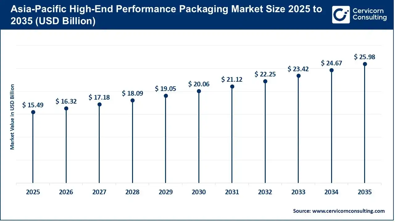
The Asia-Pacific high-end performance packaging market size was estimated at USD 15.49 billion in 2026 and is projected to hit USD 25.98 billion by 2035. Asia Pacific captured the largest share of 46% of the market in 2025, as it has a robust semiconductor production base and consistent growth in e-commerce. Specifically, Japan commenced ISES Japan 2025, where industry players like Rapidus Corporation and Preferred Networks (building MN-Core™ AI chips) addressed how Japan's local manufacturing fosters dependency on tight synergy between leading-edge logic and advanced 2.5D/3D stacking.
China High-End Performance Packaging Market
- China is noted as a major contributor to the high-end performance packaging market in 2025, as the nation seeks localisation and the overall AI transformation. In this era, several Chinese enterprises have broadened and sped up research and pilot manufacturing for glass substrates in AI chip packaging, leading to smoother, accelerated transmission speeds and shorter client verification timelines.
What are Key Catalysts of the Fastest-Growing North America Market?
The North America high-end performance packaging market size was valued at USD 10.44 billion in 2025 and is expected to reach USD 17.51 billion by 2035. In the coming era, North America is expected to expand at a rapid rate in the market because of wider investment in domestic semiconductor manufacturing and advanced packaging capacity. Along with the presence of leading industry firms in Canada, it is experiencing growing demand for AI, 5G infrastructure, electric vehicles (EVs), defense, and healthcare.
United States High-End Performance Packaging Market
- United States is predicted to witness rapid expansion in the market, as the government encourages it via funding for local semiconductor operations and massive domestic investments in flip-chip, fan-out, and embedded-die packaging. With a focus on CPO, the nation's hyperscalers and major IDMs are highly looking for local sourcing to lower reliance on overseas assembly risks and secure critical backend capabilities.
Segmentation Analysis
Packaging Type Analysis
Flip-Chip Packaging: The flip-chip packaging segment held a dominant share of 28% of the market in 2025, due to its superior performance, high interconnection density, and excellent thermal management. Moreover, the global developers of this packaging emphasised reducing bump/pillar pitches and optimizing underfill materials to manage increased thermal dissipation pressures.
The 2.5D packaging segment registered notable expansion in 2025, supported by its heterogeneous integration and resolving Moore’s Law scaling concerns. It has wider use in high-density FPGAs, like the Xilinx Virtex 7 2000T, to bring together massive logic fabrics and transceiver modules.
High-End Performance Packaging Market Share, By Packaging Type, 2025 (%)
| Packaging Type |
Revenue Share, 2025 (%) |
| 2.5D Packaging |
24% |
| 3D Packaging |
17% |
| Fan-Out Wafer-Level Packaging |
16% |
| Flip-Chip Packaging |
28% |
| System-in-Package (SiP) |
15% |
3D Packaging: The 3D packaging segment is anticipated to expand fastest during 2026-2035, propelled by a surge in demand for higher computing density, shorter interconnects, and modern AI processor architectures. As per the study, the market is transforming industrial repeatability, shorter production runs, on-demand customization, and expedited structural prototyping.
Packaging Technology Analysis
Through-Silicon Via (TSV): The Through-Silicon Via (TSV) segment led with 26% share of the market in 2025, driven by its advanced role in high-bandwidth memory and a rise in multi-die and 3D integrated circuits (3D ICs) demand for TSVs. This technology is significantly tiny and layered tightly within complicated 3D structures, which can find physical defects during fabrication.
The chiplet integration segment is projected to witness a lucrative share in the coming years, supported by its elevated manufacturing yield and remarkable economic improvement. Recently, Siemens' Innovator3D IC™ received the "Packaging: Design" award at the 2026 Chiplet Summit for speeding up the heterogeneous integration of ASICs and memory chiplets.
High-End Performance Packaging Market Share, By Packaging Technology, 2025 (%)
| Packaging Technology |
Revenue Share, 2025 (%) |
| Through-Silicon Via (TSV) |
27% |
| Chiplet Integration |
24% |
| Wafer-Level Packaging |
19% |
| Fan-Out Packaging |
16% |
| Hybrid Bonding |
15% |
Hybrid Bonding: The hybrid bonding segment is forecasted to be the fastest-growing during 2006-2035, led by tighter interconnect pitches, higher bandwidth, and enhanced integration of stacked dies. Continuous breakthroughs are pushing segmental growth, including Intel's latest unified Foveros Direct 3D hybrid bonding into its high-volume Xeon 6+ server platform, and AMD's CDNA 5 architecture leverages 3D hybrid-bonded compute dies.
Packaging Material Analysis
Organic Substrates: The organic substrates segment captured a major share of 34% of the market in 2025, due to their substantial benefits in cost, versatility, and production. Along with their broader application in diverse sectors, industry players have introduced coreless organic interposers that enhance thermal and electrical conductivity, along with miniaturization.
The mold compounds and encapsulants segment is estimated to grow at a significant rate in the predicted timeframe, fueled by their increased mechanical, thermal, and electrical protection for different devices. Along with their higher affordability in production, liquid molding compounds (LMCs) are widely employed in Fan-Out Wafer-Level Packaging (FO-WLP) and Panel-Level Packaging (PLP) to bolster supreme flowability.
High-End Performance Packaging Market Share, By Packaging Material, 2025 (%)
| Packaging Material |
Revenue Share, 2025 (%) |
| Organic Substrates |
34% |
| Silicon Interposers |
25% |
| Glass Substrates |
8% |
| Mold Compounds and Encapsulants |
18% |
| Underfill and Die-Attach Materials |
15% |
Glass Substrates: The glass substrates segment is projected to expand rapidly during the forecast period, supported by research and development into improved dimensional stability and high-density interconnects. Other key areas looking for prominent advances mainly cover recently showcased co-development of electrical TGVs and optical waveguides on the same glass core, allowing low-loss optical transmission and consolidating electronic/photonic routing for HPC computing.
Application Analysis
Artificial Intelligence and High-Performance Computing: The artificial intelligence and high-performance computing segment led with 32% share of the market in 2025 and is expected to grow fastest, driven by faster scale-up of AI models, necessitating multi-die and stacked architectures to control huge workloads. The market also includes machine learning models and co-packaged optics (CPO), as they drastically boost data transfer speeds between networking switches and compute engines.
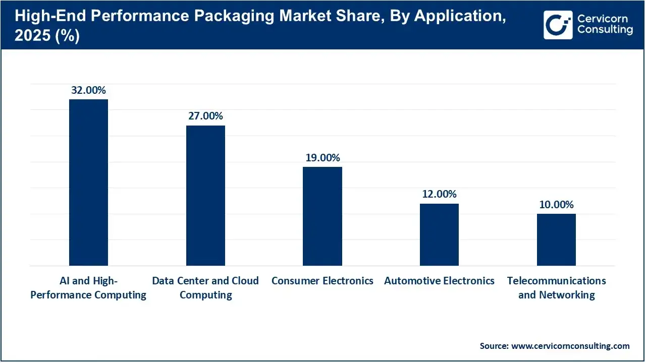
The data center and cloud computing segment held a notable share of the market in 2025, led by expansion of generative AI training and industrial-scale inference, which move towards transformative accelerators, GPUs, and custom ASICs. Moreover, the industry enabled custom logic, memory, and specialized accelerator dies to be merged and met within one integrated package for outstanding yield and cost management.
Recent Developments
- October 2026: Aeropowder, a UK-based sustainable materials firm, unveiled its PluumoPlus thermal packaging line to U.S. customers, with a new 2-8°C insulated mailer for the U.S. specialty pharmacy industry.
- September 2026: Samsung Electro-Mechanics announced the rollout of next-generation semiconductor package substrates to assist AI accelerators, data centers, and autonomous fueling performance at KPCA Show 2026.
- July 2026: Cadence Design Systems Inc. launched the AuraStack AI Super Agent on Cadence Allegro AI Studio, the world’s first agentic AI platform for printed circuit board (PCB) and advanced packaging design.
- May 2026: Advanced Semiconductor Engineering, Inc. (ASE) explored the development of an industry-first automated 310mm × 310mm panel-level packaging production line, with expansion of its leadership in next-generation advanced packaging technologies.
- April 2026: India introduced its first advanced 3D semiconductor packaging unit in Odisha, specifically for AI, 5G, and defence tech.
Key Companies
Segments Covered
By Packaging Type
- 2.5D Packaging
- 3D Packaging
- Fan-Out Wafer-Level Packaging
- Flip-Chip Packaging
- System-in-Package (SiP)
By Packaging Technology
- Through-Silicon Via (TSV)
- Chiplet Integration
- Wafer-Level Packaging
- Fan-Out Packaging
- Hybrid Bonding
By Packaging Material
- Organic Substrates
- Silicon Interposers
- Glass Substrates
- Mold Compounds and Encapsulants
- Underfill and Die-Attach Materials
By Application
- Artificial Intelligence and High-Performance Computing
- Data Center and Cloud Computing
- Consumer Electronics
- Automotive Electronics
- Telecommunications and Networking
By Region
- Asia-Pacific
- North America
- Europe
- Latin America
- Middle East and Africa
