
Content
High-End Performance Packaging Market to Reach USD 56.47 Billion by 2035, Driven by AI and Advanced Semiconductor Integration


High-End Performance Packaging Market Insights
The high-end performance packaging market size was valued at USD 33.68 billion in 2025 and is projected to surge USD 56.47 billion by 2035, growing at a CAGR of 5.3% during the forecast period of 2026-2035.
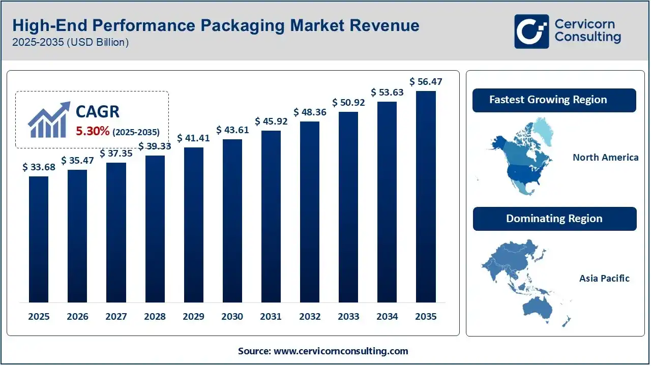
Asia Pacific registered dominance in the market, supported by its semiconductor manufacturing, assembly, and packaging ecosystem, whereas North America is anticipated to witness rapid expansion in the coming years due to expansive investment in domestic semiconductor production.
The exploration of high-performance packaging (HEPP) covers a modern semiconductor technology, which connect and secure several integrated circuits, or chiplets by leveraging high I/O density, i.e. 16 or more I/Os per mm² and fine pitch, i.e. 130 μm or less. The overall market growth is primarily propelled by a rise in demand for AI GPUs, Application-Specific Integrated Circuits (ASICs), and HBM (High Bandwidth Memory) integration. Additionally, the continuous combination of tiny, unique dies on one package and expedited expansion in Advanced Driver Assistance Systems (ADAS) and high-density vehicle compute modules fuels demand for 2.5D and 3D packaging.
The global market progression is increasingly promoting glass substrates in manufacturing that offer superior thermal performance, minimal signal loss, and vast area integration. Another subsidiary trend is a shift to panel-level packaging (PLP) from conventional circular wafers to rectangular panels to minimize expenses and boost package sizes.
AI Assistance
Most of the advances across packaging have been driven by the consistency and broader use of AI solutions, while AI-enabled designs support modelling and resolving intricate thermal crosstalk, power delivery losses, and mechanical pressure. Along with this, the market is transforming yield and quality intelligence by employing machine learning models, tracking non-conformance patterns, inspection outcomes, and process changes across multi-vendor supply chains. On the other hand, AI industries are advancing tools simulating vertical power delivery structures and co-packaged optics (CPO) integration to crucially eliminate energy loss and manage higher thermal loads in AI data facilities. However, many of the packaging equipment producers are inserting Domain-Specific Language Models (DSLMs) and multi-agent AI systems into major hardware, enabling workers to immediately query complex machinery manuals, automatically estimate maintenance, with perfect rapid SKU changeovers.
Regional Overview
Asia Pacific Was Dominant in the Market in 2025
In 2025, Asia Pacific held the largest share of 45% of the high-end performance packaging market, driven by steps in localization and faster research and pilot manufacturing for glass substrates in AI chip packaging. Specifically, Taiwan expanded as a global hub for foundry-driven advanced packaging (TSMC), while South Korea promoted memory packaging and HBM integration. At the same time, the Indian market pursued a goal of glass panels and 3D heterogeneous integration modules to assist aerospace, defense, and AI processes. More innovative ideas from China have broadened the adoption of multi-chiplet packaging to connect mature nodes and match the performance of tighter nodes.
North America is predicted to be the fastest-growing region
Moreover, North America is predicted to be the fastest-growing region during 2026-2035, fueled by the presence of advanced packaging capacity and ongoing government incentives across the packaging industry. Recently, the region hosted an event called PACK EXPO International 2026, which showcased how unified, fully connected packaging lines are enhancing line versatility, waste reduction, and throughput for North American developers. Meanwhile, Canada’s progression is primarily driven by the involvement of high-speed communications and data centers, pushing the use of low-loss, high-frequency packaging approaches. Alongside this, the nation has well-qualified technical staff and planned physical proximity, particularly for specialized high-end OSATs (Outsourced Semiconductor Assembly and Test) and groundbreaking packaging.
High-End Performance Packaging Market Segmental Outlook
| Market Segment | Leading Segment | Key Growth Factor |
| By Packaging Type | Flip-chip Packaging | Led by its advanced use in high-performance processors, graphics chips, and networking devices. |
| By Packaging Material | Organic Substrates | Driven by their broader application in advanced semiconductor packages. |
| By Application | AI and high-performance computing | Propelled by a surge in demand for high-bandwidth memory and advanced processor integration. |
Emerging Trends
- Innovative & Modern Materials: Nowadays, many brands are implementing premium packaging, which heavily depends on mono-material cartonboard structures combined with advanced, water-based functional coatings that lead to moisture, aroma, and grease resistance.
- Embracing Lightweight Solution: In 2026, the packaging industry is seeking to promote lightweight luxury and industrial minimalism, which possess ultra-clean chrome envelopes and highly recyclable anodized aluminum and serve as a milestone of the latest prestige aesthetics.
- Implementation of Regulations: By considering global anti-PFAS guidelines and strict Extended Producer Responsibility (EPR) laws, the market is increasingly integrating digital watermarks, NFC tags, and encrypted QR codes. Also, this preserves cryptographic authentication and supports the rollout of engaging, post-purchase consumer brand ecosystems.
Future Outlook
During 2026-2035, the high-performance packaging market progression will demonstrate 3D copper-to-copper (Cu-Cu) hybrid bonding that gives ultimate power efficiency and ultra-high vertical I/O density, with massive scale-up. Meanwhile, recent advances are pushing the adoption of glass-based packaging modules, as they offer superior dimensional stability, flatness, and thermal performance and enable stringent interconnect pitches. To overcome data risks in AI data centre optical networking will propel early-stage commercial velocity for Co-Packaged Optics (CPO) via insertion of optical engines directly into the compute package employing Through-Silicon Vias (TSVs) and microbumps, systems can eliminate the efficiency challenges of conventional copper routines. Simultaneously, significant market expansion is sustained by the consolidation of key firms, including Intel, TSMC, Samsung, SK Hynix, and Micron. This is enabled by a single AI accelerator package that currently covers more than seven distinct vendors.
Segments Covered in the Report
By Packaging Type
- 2.5D Packaging
- 3D Packaging
- Fan-Out Wafer-Level Packaging
- Flip-Chip Packaging
- System-in-Package (SiP)
By Packaging Technology
- Through-Silicon Via (TSV)
- Chiplet Integration
- Wafer-Level Packaging
- Fan-Out Packaging
- Hybrid Bonding
By Packaging Material
- Organic Substrates
- Silicon Interposers
- Glass Substrates
- Mold Compounds and Encapsulants
- Underfill and Die-Attach Materials
By Application
- Artificial Intelligence and High-Performance Computing
- Data Center and Cloud Computing
- Consumer Electronics
- Automotive Electronics
- Telecommunications and Networking
By Region
- Asia-Pacific
- North America
- Europe
- Latin America
- Middle East and Africa
Empower your strategy with expert insights, purchase this premium research@ https://www.cervicornconsulting.com/buy-now/3069
Ask here for more details@ sales@cervicornconsulting.com